- 您现在的位置:买卖IC网 > Sheet目录1996 > HMP8156ACNZ (Intersil)IC VIDEO ENCODER NTSC/PAL 64MQFP
32
FN4343.5
August 20, 2009
For proper operation, power supply decoupling is required. It
should be done using a 0.1
μF ceramic capacitor in parallel
with a 0.01
μF chip capacitor for each group of V
AA pins to
ground. These capacitors should be located as close to the
VAA and GND pins as possible, using short, wide traces.
If a separate linear regulator is used to provide power to the
HMP8154/HMP8156A power plane, the power-up sequence
should be designed to ensure latchup will not occur. A separate
linear regulator is recommended if the power supply noise on
the VAA pins exceeds 200mV. About 10% of the noise (that is
less than 1MHz) on the VAA pins will couple onto the analog
outputs.
External Reference Voltage
If an external reference voltage is used, its circuitry should
receive power from the same plane as the HMP8154/
HMP8156A. The external VREF must also be stable and well
decoupled from the power plane. An example VREF circuit
using a band gap reference diode is shown in Figure 37.
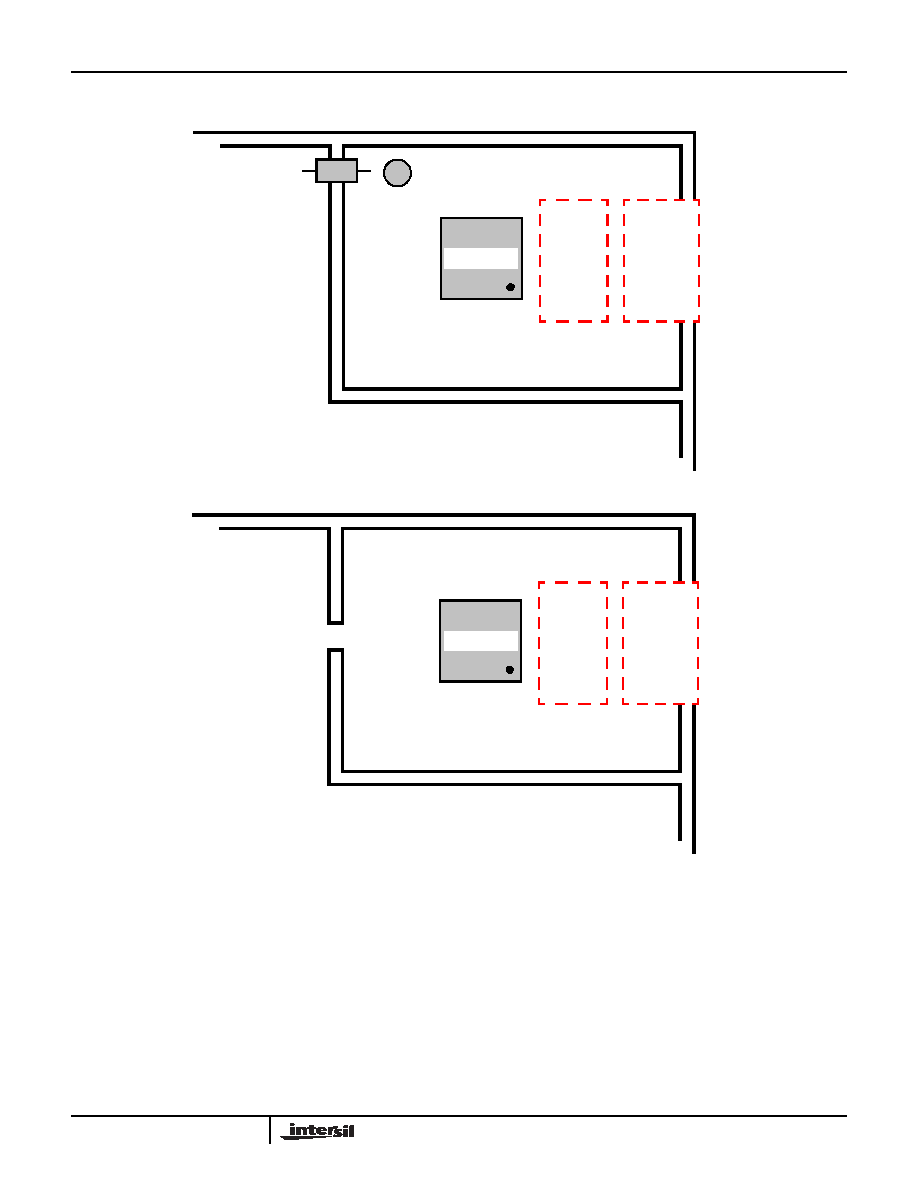
FIGURE 36A. VCC AND VAA PLANES
FIGURE 36B. COMMON GROUND PLANE
FIGURE 36. EXAMPLE POWER AND GROUND PLANES
LP
VCC
VAA
FERRITE
BEAD
BULK AREA
CAPACITOR
8154/8156A
PCB
ANALOG
FILTERS
CONN.
LP
GND
8154/8156A
PCB
ANALOG
FILTERS
CONN.
HMP8154, HMP8156A
发布紧急采购,3分钟左右您将得到回复。
相关PDF资料
HSP45102SC-40Z
IC OSC NCO 40MHZ 28-SOIC
HSP45106JC-33Z
IC OSC NCO 33MHZ 84-PLCC
HSP45116AVC-52Z
IC OSC NCO 52MHZ 160-MQFP
ICL7109EPL+
IC ADC 12BIT 3-ST 40-DIP
ICM7217AIPI
IC OSC UP/DWN CNTR 2MHZ 28-DIP
ICM7217CIPI
IC OSC UP/DWN CNTR 2MHZ 28-DIP
ICM7242IPA
IC OSC BINARY CTC 13MHZ 8-DIP
ICM7250IWE+T
IC OSC BINARY CTC 15MHZ 16SOIC
相关代理商/技术参数
HMP8156CN
制造商:Rochester Electronics LLC 功能描述:- Bulk
HMP8156EVAL1
制造商:INTERSIL 制造商全称:Intersil Corporation 功能描述:NTSC/PAL Encoders
HMP8156EVAL2
制造商:Rochester Electronics LLC 功能描述:- Bulk
HMP8170
制造商:INTERSIL 制造商全称:Intersil Corporation 功能描述:NTSC/PAL Video Encoder
HMP8170_03
制造商:INTERSIL 制造商全称:Intersil Corporation 功能描述:NTSC/PAL Video Encoder
HMP8170CN
制造商:INTERSIL 制造商全称:Intersil Corporation 功能描述:NTSC/PAL Video Encoder
HMP8170EVAL1
制造商:INTERSIL 制造商全称:Intersil Corporation 功能描述:NTSC/PAL Video Encoder
HMP8171
制造商:INTERSIL 制造商全称:Intersil Corporation 功能描述:NTSC/PAL Video Encoder